
Photonics testing requires precise and repeatable optical coupling and, where applicable, electrical or RF probing of the device under test. The requirements depend on the photonic device, its optical interfaces, the measurement task, and the stage of development or production. Grating, edge, and trench coupling can require different positioning and alignment strategies, while optical and electro-optical characterization, including RF measurements, require suitable instrumentation and coordinated measurement workflows.
SmarAct addresses these requirements with a modular testing architecture for photonic integrated circuits (PICs). The architecture combines functional building blocks for wafer and die positioning, pre-alignment, metrology and feedback, fast optical alignment, and measurement integration. These building blocks are selected and configured according to the application, allowing individual components to be used independently or combined into an automated test workflow. This approach supports setups ranging from R&D and device characterization to small-batch testing, with scope for integration into production test environments.
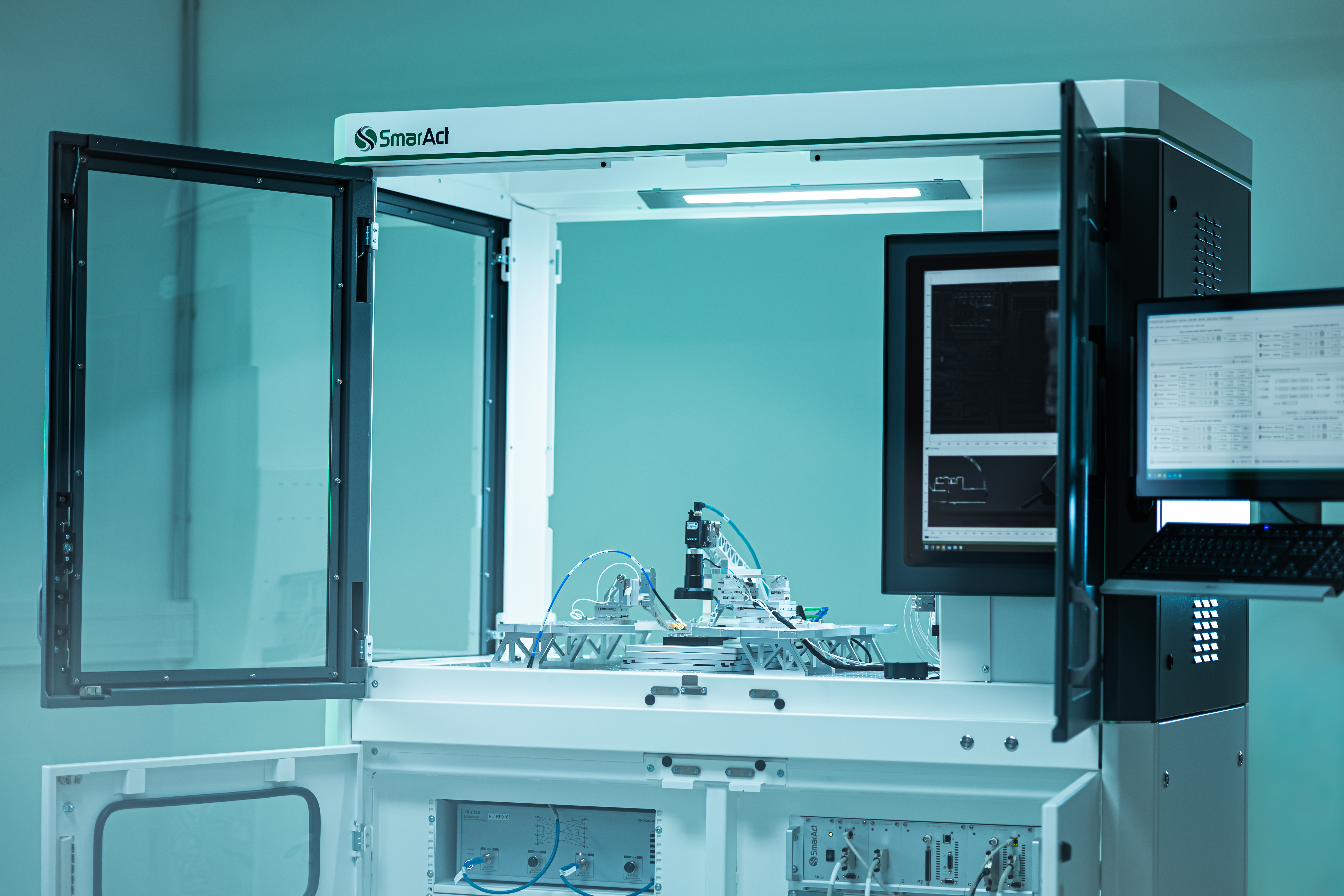
Figure 1 Modular setup for automated electro-optical PIC characterization, integrated into an enclosure.
Building the Photonics Test Chain
Wafer and sample stages position individual dies, devices, or measurement sites within reach of the test interfaces. Options range from compact XY stages to customized wafer stages with application-specific travel ranges, access geometries, and integrated metrology.
For optical access, positioning and pre-alignment algorithms bring fibers, fiber array units (FAUs), probes, or optical heads into the required position and orientation relative to the device. Different configurations provide lateral positioning, XYZ motion, or up to six degrees of freedom. Tool and pivot calibration establish the working position and orientation of the optical interface and its effective pivot point, enabling accurate multi-axis alignment.
Integrated metrology systems can provide local distance, height, and surface information for the subsequent alignment process. Capacitive sensing or optical distance measurement, for example, can support controlled approach and height-sensitive optical coupling. For wafer-level applications, surface-topography measurements can provide reference data for subsequent positioning and test processes.
Once the optical interface has been approached, multiple options for coupling characterization and fine alignment are available. Using piezo-based scanner positioners, position-associated coupling efficiencies can be quickly captured using the motion controllers firmware features. These measurements may be used for closed-loop optimization subsequently. For lateral 2D alignment, the scanner positioners enable fast coupling optimization based on tight control loops directly on the motion controller.
For optimization procedures which do not yet have a controller-integrated option – as multidimensional optimization across different controllers – SmarAct's Development Environment offers methods to perform the optimization with flexible gradient search routines.
The architecture can accommodate application-specific optical, electro-optical, and RF instrumentation through open software interfaces. External hardware can be integrated using plug-ins or Python modules, including existing modules provided by instrument manufacturers. SmarAct's Development Software can coordinate motion, alignment routines, instrument control, measurement sequences, visualization, and data acquisition within a common workflow. This allows external measurement equipment to be integrated alongside SmarAct motion and alignment technology.
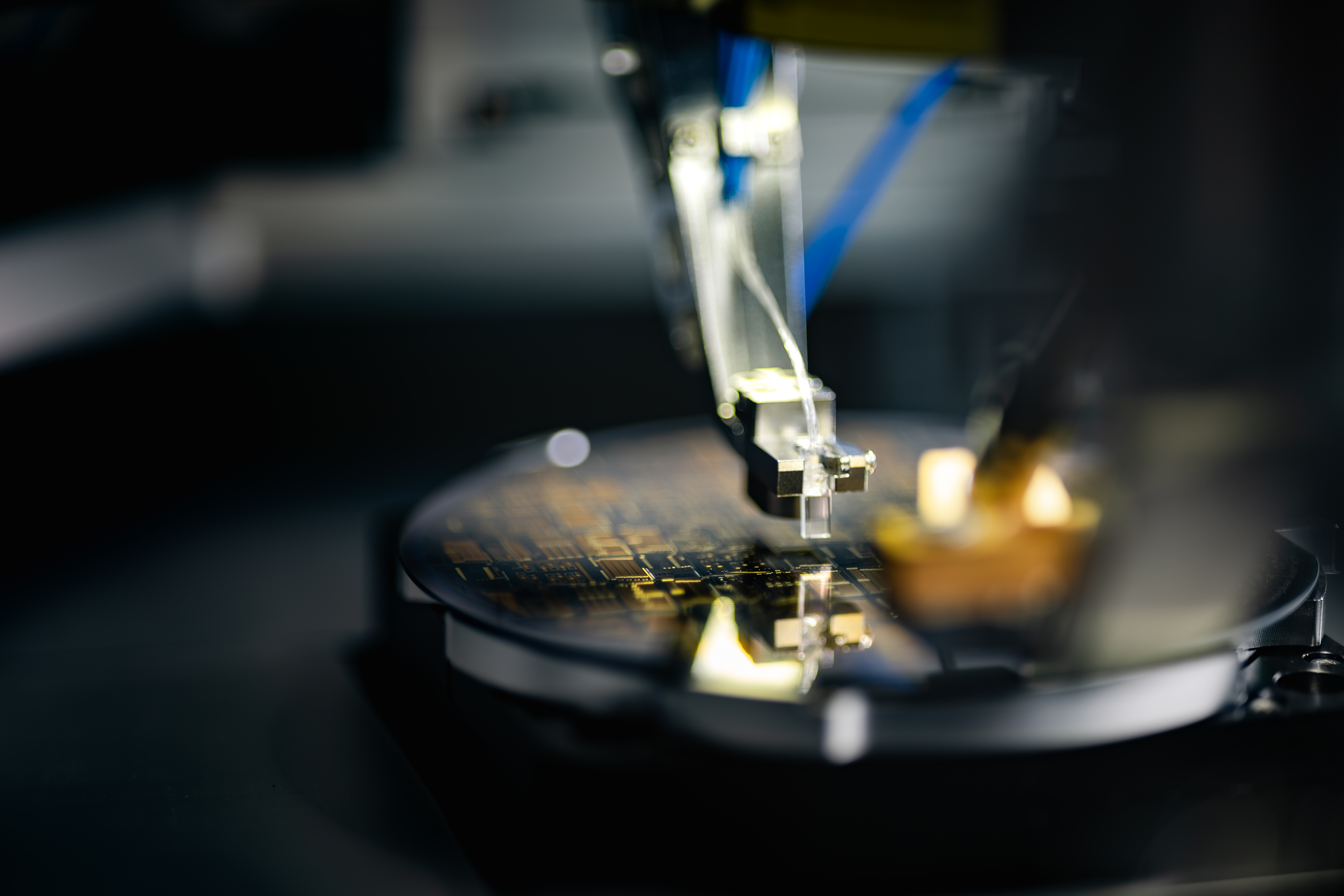
Figure 2 Example configuration: Electro-optical RF characterization of LTOI Mach-Zehnder modulators at wafer level.
Automated Electro-Optical Wafer-Level Testing
A practical implementation of this architecture was demonstrated by SmarAct together with Luxtelligence and Anritsu. The setup performs automated wafer-level alignment, optical coupling, and electro-optical characterization of LTOI Mach–Zehnder modulators from Luxtelligence. An Anritsu ShockLine™ MS46524B vector network analyzer captures the electro-optical response, while SmarAct provides the motion modules, alignment algorithms, and control technology.
The workflow includes system calibration to establish the relevant tool and coordinate relationships, followed by wafer navigation, device localization, optical alignment, and measurement. The optical interface is then positioned and aligned to the selected device, with fine-alignment routines optimizing the optical coupling. Electrical probing and the vector network analyzer complete the measurement chain for characterizing the device’s electro-optical frequency response. SmarAct’s Development Software aims at connecting the individual steps through reusable process blocks for device control, alignment, measurement, visualization, and data handling.
The demonstrator illustrates the central idea of the modular architecture: the device, optical interface, instrumentation, and required level of automation determine the configuration. SmarAct components can be used as individual building blocks, combined into functional subsystems, or integrated into a coordinated test architecture together with customer and third-party equipment. This gives machine builders, system integrators, and photonics manufacturers the flexibility to develop application-specific test equipment while retaining control over the choice of components, instrumentation, and level of automation.