

The modification of material properties such as surface characteristics, manipulating electronic and magnetic behavior, and optical attributes has reached sub-atomic scales. Quantum mechanical systems and quantum effects are at the forefront of research and development, finding pathways into a wide range of applications. Suitable analysis methods are under development, while established techniques are continuously improved and adapted to meet the growing demands for increased precision and stability.
Smaract systems allow for precise sample manipulation while being highly customizable, increase complexity while remaining compact and are available for use in extreme environments, such as high magnetic fields, ultra-high vacuum, cryogenic conditions, and high-intensity radiation fields. These advancements enable deeper exploration of the Nano, Pico, and Quantum world, ensuring that new effects can be reliably detected and harnessed.
A broad product portfolio, comprehensive in-house manufacturing depth, intrinsic innovative strength, and extensive development expertise, nearly all use cases, and highly specialized applications can be addressed. OEM solutions can be conceived, implemented and realized with all technical aspects considered.
Whether it is high-resolution 3D printing, ultra-precise sample handling, electron or scanning probe microscopy, nanoindentation, nanoprobing, spectroscopy, diffractometry or quantum computing and sensing, or nanometer-resolution metrology, industrial and OEM customers as well as research facilities rely on SmarAct’s expertise.

Precision Solutions, Engineered Together
At SmarAct, we know that every advanced research setup comes with its own challenges, constraints and goals. That is why we do more than provide high-precision positioning components — we work closely with you to understand your application, your workflow and your technical environment.
Whether you need a ready-to-use micro- or nanomanipulator, a modular multi-axis sample handling system, or a fully customized positioning platform, SmarAct is your partner from the first idea to the final integration.
With application-focused consulting, flexible system concepts and deep engineering expertise, turning complex motion and integration challenges into practical, future-ready solutions.
Multi-axis Sample Handling Systems & Manipulators

- Wide variety of ready-to-use micro- and nanomanipulators as well as complete manipulation systems, supported by application-focused consulting to match each setup to the customer’s experimental workflow.
- Modular system concepts that enable flexible configuration, future extensions and efficient adaptation to changing research requirements.
- Microrobotic solutions for precise multi-axis sample handling, developed in close collaboration with customers to address complex motion and integration challenges.
Highly Specialized Customized (OEM) Systems & Platforms
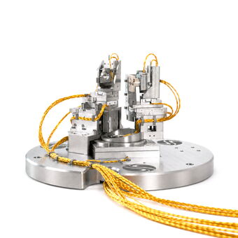
- Collaborative design, mechanical layout and sizing of complex multi-axis positioning systems, tailored to the customer’s application, interfaces and performance requirements.
- Kinematic modeling to support reliable motion, optimized axis arrangements and precision throughout the system architecture.
- Integration into existing environments such as microscopes, vacuum chambers, beamlines or laboratory platforms, with engineering support from concept to implementation.
- Retrofitting and adaptation of established systems to extend functionality, improve precision or add a wider range of new capabilities with minimal disruption.
Relevant Technical Application Fields & Use Cases
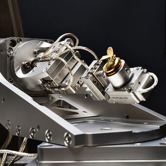
- Electron microscopy applications including SEM, TEM, STEM and CryoSEM, supported by precision positioning solutions adapted to demanding imaging and in-situ workflows.
- Spectroscopy and analytical methods such as nanoARPES, XRD and EDS, where reliable alignment and stable motion contribute to reproducible measurement results.
- Scanning probe microscopy including AFM and STM, requiring nanometer-level positioning, mechanical stability and application-specific system design.
- Nano Computer tomography setups supported by precise sample positioning and motion solutions for accurate imaging, alignment and measurement workflows.
- Quantum computing and sensing applications requiring close engineering collaboration to meet demanding requirements for precision, materials, operation and system integration.
- Nanoindentation workflows supported by accurate positioning and controlled motion for advanced material characterization and inspection tasks.
- Electrical and tactile probing applications enabled by precise multi-axis manipulation, reliable contact control and integration into electron microscopy or test environments.
Environment, Material & Precision Options in Detail

- Solutions, customized for applications ranging from standard laboratory setups to UHV environments down to 10⁻¹¹ mbar.
- Configurations, engineered to support reliable precision motion under demanding thermal conditions, room temperature to cryogenic environments.
- Non-magnetic material options for sensitive applications, magnetic-field environments and other setups where magnetic interference must be minimized.
- Nanometer-resolution positioning capabilities to support precise and repeatable motion alignment, probing and measurement in advanced research and inspection systems.
- Interferometric cryogenic sensor for applications requiring high-precision position feedback and reliable metrology performance at very low temperatures.
Application Examples
Enhancing X-ray Dark-Field Imaging with Tunable Interferometry
X-ray dark-field imaging is a novel technique that enables visualization of structures beyond the conventional resolution limit of X-ray radiography and tomography. This example shows a dual phase grating interferometer (DPGI), which generates Moiré patterns on a X-ray detector. Changes in the pattern contrast caused by the sample provide information on small-angle scattering induced by sub-micrometer features. A key advantage of the DPGI is its tunability: adjusting the distance between the two gratings shifts the sensitivity to different feature sizes, allowing sub-micrometer characterization of centimeter-scale samples. In this setup, four SmarAct stages control grating alignment, phase stepping, and inter-grating distance, enabling precise alignment and tunable system sensitivity.


4D Scanning Transmission Electron Microscopy
4D Scanning Transmission Electron Microscopy (4D-STEM) is a powerful technique for mapping material properties such as crystal symmetry, lattice parameters, and strain. A focused electron beam scans an electron-transparent sample, while a diffraction pattern is recorded at each position, enabling high-resolution analysis. Adaptable to standard SEMs, 4D-STEM is well suited for thin samples such as 2D materials and 2D-like Van der Waals heterostructures, offering sub-nanometer resolution over scan areas of several mm². In this example, an in-house system integrated a SMARPOD 110.45.2 for six-degree-of-freedom sample positioning and a SmarAct linear stage to precisely adjust the camera length, enabling fast, high-quality data acquisition.
The Art of SEM Imaging
The Leipzig Panometer presents immersive 360° panoramas inside a former gasometer, created by artist Yadegar Asisi. From January 2019 on, the exhibition “Carolas Garden” has taken visitors into the microcosm, showing flowers and insects from the perspective of a grain of pollen, enlarged one hundred times. Scientific photographer Stefan Diller contributed by producing scanning electron microscopy (SEM) images of a honey bee and a chamomile blossom. These images form one of the world’s largest cycloramas (110 × 32 m), requiring extremely high image resolution. Conventional macro photography was insufficient, so a TESCAN MIRA3 FE-SEM equipped with a multi-detector setup and a SmarAct eight-axis SEM piezo stage was used. The SmarAct stage enabled nanometer-precise positioning and tile acquisition to create the final stitched panorama.


6D System for the µRobotex Platform
The μRobotex platform is a facility dedicated to characterization and microassembly of micro/nanosystems with dimensions below 10μm [1]. It is located at the École nationale supérieure de mécanique et des microtechniques (ENSMM) in Besançon and is managed by the AS2M department of the FEMTO-ST Institute.
The μRobotex team asked SmarAct to build a 6D system with position feedback for tool handling in a scanning electron microscope. The positioning system consists of two 3D subsystems mounted onto each other. The first consists of two SLC Series and one SLL Series stage, the later of two goniometers and a rotation stage in order to be able to manipulate nano-tools in six degrees of freedom.
The µRobotex team commands the positioning system via their own real-time control system.


